PSN SSB modulator
To realize SSB modulation with low distortion, I tried to construct PSN SSB modulators.Principle
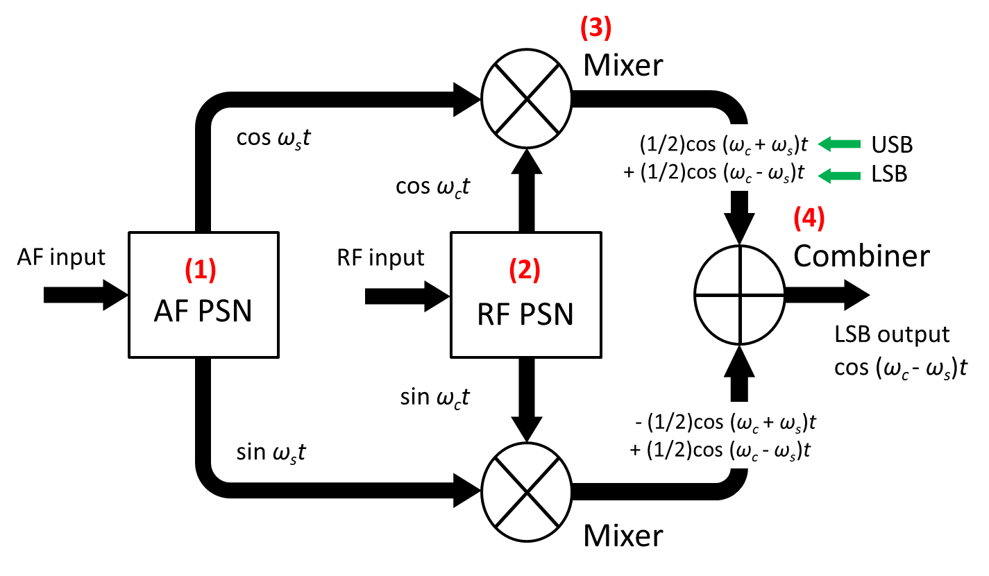
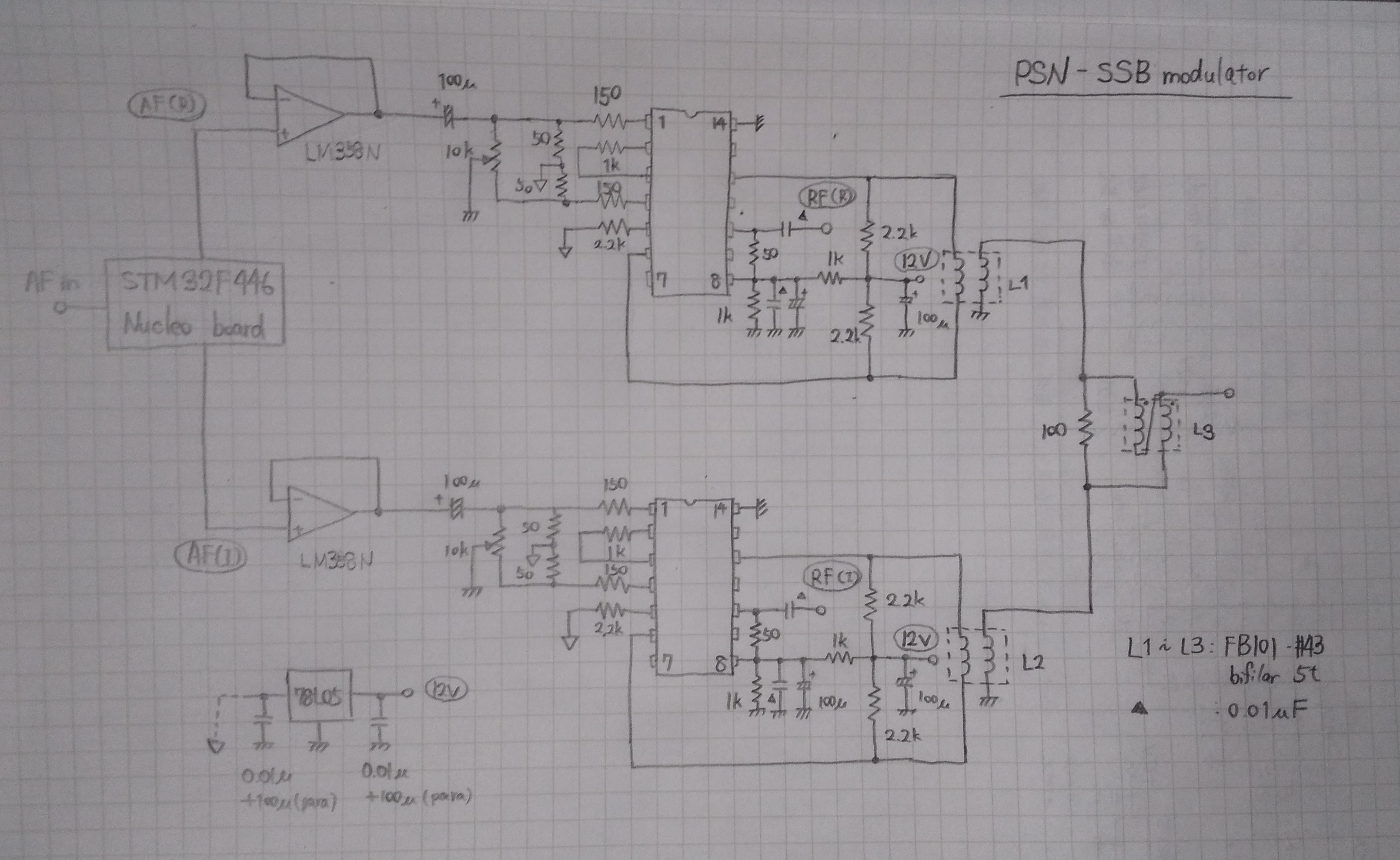
Here is detail explaination (in Japanese).As a schematic diagram shown in below figure, single side band (SSB) signal is generated with orthogonal signals of AF and RF ((1) and (2)), by multiplying them respectively (3) and adding their outputs (4). In order to realize sufficient side band suppression in practice, it is necessary to gerate PSN signals with good orthogonality and to employ symmetric mixer and combiner. Here, each component for (1) to (4) are as follows.
Configuration
(1)Generation of AF PSN signal
PSN signals are generated with the FIR filter embedded in a microcomputer STM32F446RE. You can download files from here. Detail is explained in here.(2)Generation of RF PSN signal
An RF PSN signal is generated by dividing second harmonic frequency into desired frequency. The circuit diagram is shown below. The input signal is generated directly from the Si5351A. If the input frequency exceeds the upper limit frequency of the logic IC, the orthogonality becomes lower and necessary side band suppression won't be obtained. Since the input frequency is twice the desired frequency, it is necessary to select logic ICs with relatively high operation speed.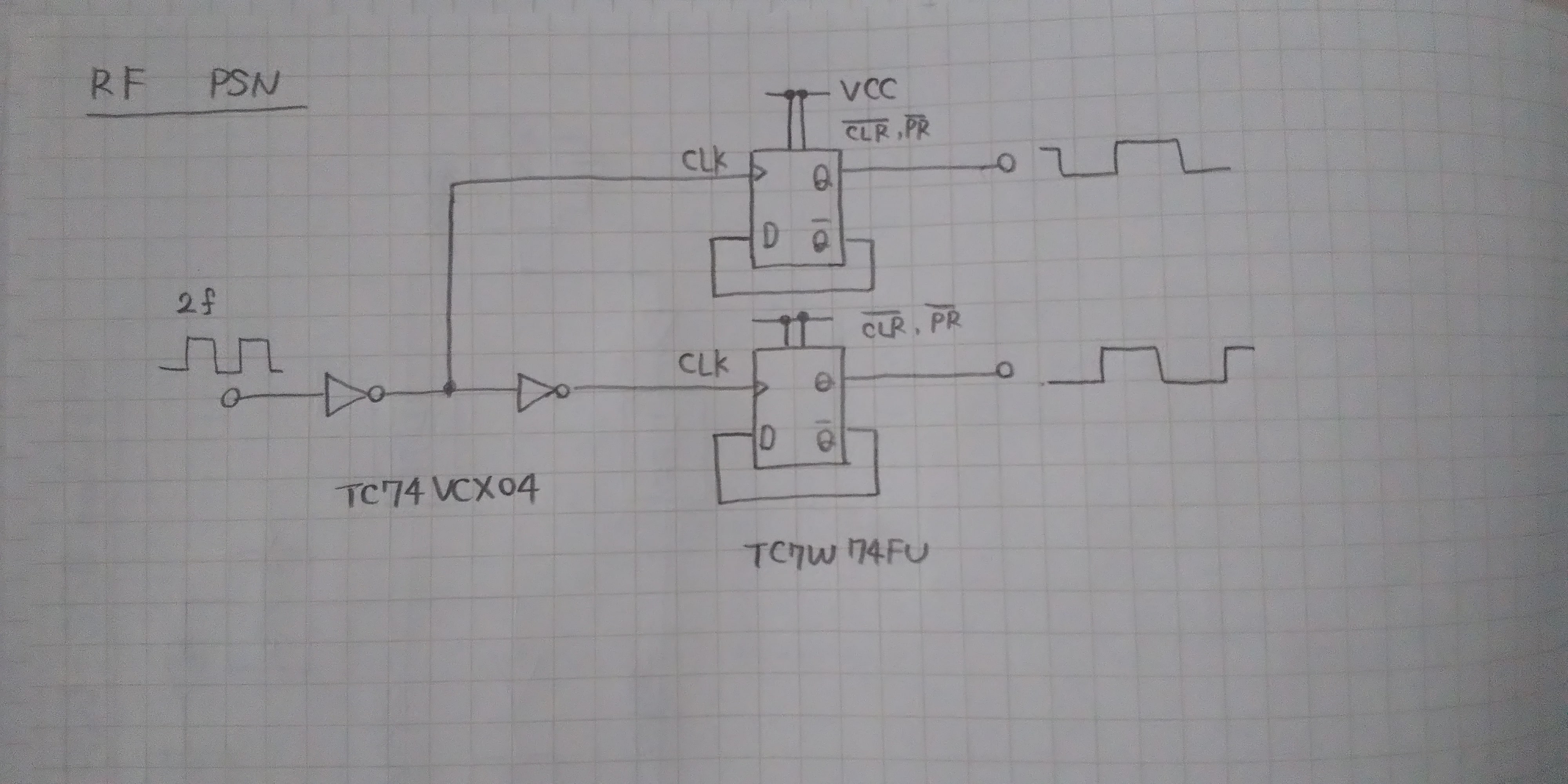
(3) Mixers
To supress carrier leak enough to construct without external filters, I employed NJM1496D. Carrier null-point is caliblated by variable resistace. Since it is sensitive to fluctuations in the power supply voltage, it is desirable to make supply voltage stable. The circuit and its characteristics are as follows. The carrier leakage is very small (<-60dB).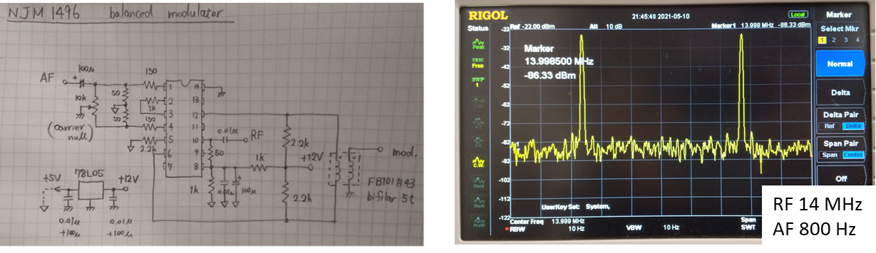
(4)Combiner
Wilkinson combiner with FB101#43 is used here.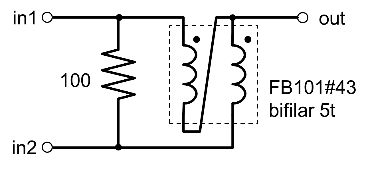
This time, I construct a PSN SSB modulator with discrete components. However, Since there are ICs for quadrature modulation, I would like to use them near future.
Characteristics
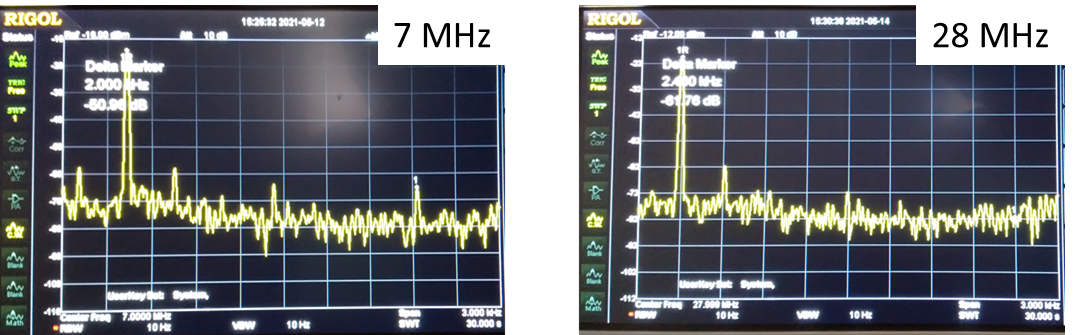
Here, wiring becomes complicated, but SSB modulation with sufficient side band supression is obtained.The picture show the output spectrum for 7MHz and 28MHz, respectively. Although it depends on the input signal level, relative amplitude of unneccesary side band is less than -50dB with peak power operation, which is sufficient for HF bands. By listening to the modulated signal and comparing with the conventional filter modulator, you can see low distortion signal is realized.
ラジオの音声で変調を確認したところ、素直なSSB変調が得られました。
— JR2BMU/1 (@jr2bmu) May 12, 2021
ただしFIRフィルタの特性により低域が減衰気味、今後改善の余地が残ります。 pic.twitter.com/b2EabQ4UeM